

The semiconductor industry has a visibility problem. As chipmakers stack silicon wafers like high-rise apartments and wire chiplets into dense urban grids, the tools they rely on to spot defects are increasingly flying blind. Enter QuantumDiamonds, a Munich startup that believes the solution lies in synthetic diamonds and the strange physics of quantum mechanics.
On July 9, 2026, the company announced €91 million in combined financing—€15 million in fresh equity and €76 million in state aid approved under Europe's newly minted Chips Act. It's a funding structure that tells two stories at once: venture capital betting on commercial viability, and Brussels betting on sovereignty. World Fund, the climate-focused investor, led the equity round, joined by Bayern Kapital and a roster of returning backers including IQ Capital, Earlybird, and First Momentum. The company declined to share its valuation, as startups in sensitive sectors often do.
The state backing, formally blessed by the European Commission on June 23, underwrites a €152 million production facility in Munich that QuantumDiamonds first unveiled last December. Sections of the plant are slated to open in 2026—a timeline that speaks either to confidence or ambition, depending on whom you ask.
The Physics Underneath
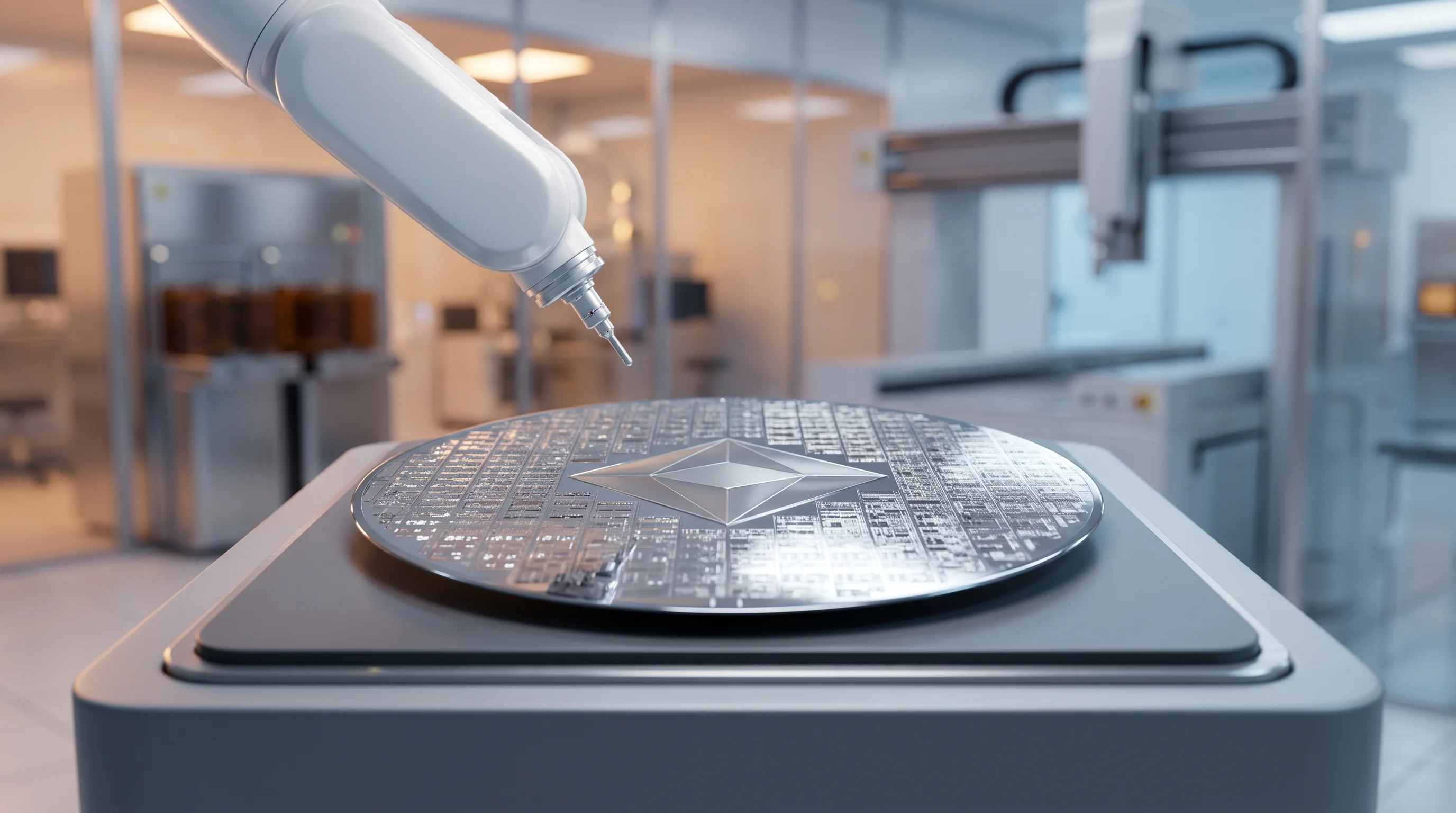
What QuantumDiamonds sells is unusual enough to require some unpacking. The core technology, Quantum Diamond Microscopy, exploits defects—nitrogen atoms lodged in synthetic diamond lattices—to visualize magnetic fields generated by electrical current flowing through chips. Point these sensors at a modern integrated circuit, and they can map current pathways buried inside multilayer packages: the 3D stacks, chiplet arrays, and through-silicon vias that define the industry's current roadmap.
Traditional optical inspection, refined over decades, struggles with these architectures. Light can't see through stacked layers with much fidelity. QuantumDiamonds claims its tools offer resolution "up to 100× smaller than traditional inspection" while covering fields of view as large as 5×5 centimeters through image stitching. The assertions come from the company itself, naturally, but two early customers have put money behind the pitch: Eurofins EAG Laboratories in California and Integrated Service Technology in Taiwan both installed systems this year.
The QDm.1 platform, launched at SEMICON Taiwan last September, is positioned as the first commercial quantum sensing tool built specifically for failure analysis. It operates at room temperature—no cryogenics required—and the company prices lab-scale units in the single-digit millions. Factory-ready inline tools, still in development, could command $10 million to $15 million per system, according to TechCrunch reporting from early July.
Chasing a Moving Target

Advanced packaging has become the semiconductor industry's fixation, perhaps out of necessity. Moore's Law hasn't died so much as gotten expensive and complicated, and chipmakers are compensating by stacking dies vertically and arranging chiplets horizontally. The resulting structures—high-bandwidth memory modules, hybrid-bonded processors—create electrical and thermal environments that legacy metrology wasn't designed to interrogate.
A June industry survey flagged hybrid bonding as the single most difficult structure to analyze and called for higher-resolution non-destructive imaging. Established inspection giants—KLA, Onto Innovation, Camtek—have all rolled out or expanded advanced packaging platforms over the past twelve months, often relying on X-ray or enhanced optical techniques. QuantumDiamonds is wagering that magnetic current imaging addresses a gap those approaches can't fully close: electrically sourced defects deep inside multilayer assemblies, invisible to photons and hard to reach without destructive cross-sectioning.
Whether that gap is real, or large enough to sustain a business, remains an open question. The company, spun out of Technical University of Munich in 2022, previously raised €7 million in seed funding back in December 2022. CEO Kevin Berghoff and CTO Dr. Fleming Bruckmaier, the co-founders, now oversee roughly 70 employees and plan to more than double engineering headcount over the next year—a hiring sprint that signals both opportunity and urgency.
Asia and the Fab Floor
QuantumDiamonds opened a regional hub in Taiwan this year and signed a memorandum of understanding with Korea's Woowon Technologies in February, moves that reflect where the action is. Taiwan and Korea together account for the majority of global advanced packaging capacity, and validation in those markets is less about geography than credibility.
The company claims on LinkedIn that nine of the ten largest chipmakers are "now engaged with us," though that phrasing is vague—engaged could mean anything from pilot testing to polite conversations. What's clearer is the near-term agenda: deliver systems to what the company describes as leading chipmakers, scale the Munich line, and push wafer-level inspection tools from lab curiosity to production readiness.
Pricing, competitive positioning, and real-world traction will come into focus as QuantumDiamonds moves from early deployments to volume production. The company has capital, regulatory tailwinds, and a handful of reference customers. Whether quantum sensing becomes standard infrastructure or remains a specialized niche depends largely on what happens in those first fab installations—and whether the magnetic signatures QuantumDiamonds can see translate into defects that matter. For now, it's a bet on physics meeting economics at a moment when chipmakers are running out of easy answers.


